When the minimum slitting width of the slitting machine is 5mm, it does face some technical challenges in precision electronic material cutting. Here are the key points to analyze and solve:
1. Technical difficulties
• Material properties
Electronic materials (such as flexible circuit boards, ultra-thin metal foils, optical films, etc.) are usually highly brittle, prone to delamination or heat sensitivity, and are prone to burrs, cracks, or delamination when cutting narrow widths.
• Equipment accuracy limitations
◦ The positioning accuracy of the tool/laser head needs to reach the micron level (± less than 1μm), and the width of 5mm is extremely sensitive to mechanical vibration and the straightness of the guide rail.
◦ Uneven slitting tension control can cause material serpentine deviations (e.g., very thin copper foil).
• Heat-affected zone (laser cutting)
When laser cutting, heat diffusion can lead to edge carbonization or micromelting (such as PI films), affecting conductivity.
2. Solution
Equipment optimization
• Highly rigid slitting mechanism
It is driven by an air-bearing spindle and linear motor, with a raster ruler with real-time feedback, to ensure that the dynamic accuracy of the tool is ≤± 2μm.
• Microtension control system
Use magnetic particle brake + high-resolution tension sensor to control tension fluctuations within ±0.1N (e.g., for 6μm lithium battery separators).
• Special knife design
◦ Diamond-coated circular knife (edge radius ≤0.1μm) reduces cutting stress.
◦ Ultrasonic vibration-assisted cutting (frequency 40kHz) reduces the risk of thin material deformation.
Process improvement
• Multi-level slitting strategy
Rough cutting (10mm wide) and then finishing (5mm) to reduce the load of a single cut.
• Low-temperature assisted cutting
Liquid nitrogen cooling (-196°C) is injected during laser cutting to control the heat-affected zone to <10μm (e.g., silicon wafer cutting).
• Dynamic visual correction
The CCD camera monitors the edge position in real time and adjusts the correction roller (accuracy ± 5μm) in a closed loop.
Material pretreatment
• UV curable coating
Apply a temporary protective layer (such as acrylate UV glue) before cutting to prevent delamination.
• Low temperature annealing
Pre-annealing of brittle materials (such as glass substrates) to release internal stress.
3. Industry application cases
• Flexible OLED screen
CO₂ laser (wavelength 10.6μm) is used to slitter 5mm wide FPC, with nitrogen purging, and the cut roughness < Ra 0.5μm.
• MLCC ceramic film
The diamond grinding wheel dicing machine achieves 4.8mm slitting and the chipping edge size < 20μm.
4. Future trends
• Ultrafast laser (picosecond/femtosecond)
The cold working mechanism avoids thermal damage and the minimum cut seam can reach the 10 μm level.
• Digital twin simulation
Predict the impact of cutting parameters on the material through virtual debugging.
If you need to further explore the cutting options for specific materials (such as graphene, liquid metal, etc.), more details can be provided for targeted analysis. The core of precision slitting lies in the collaborative optimization of "equipment-process-material".
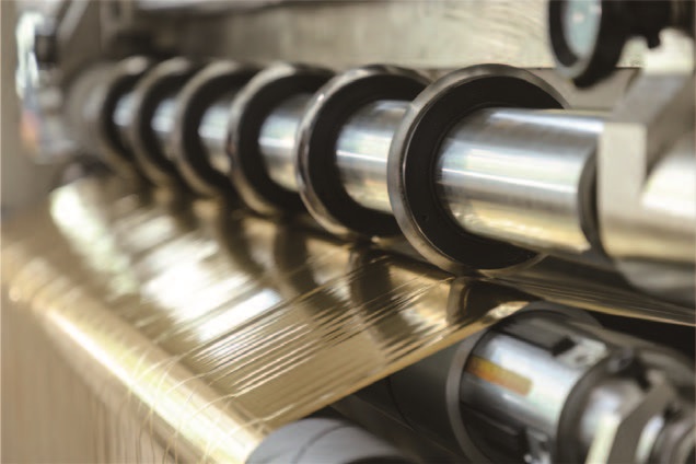
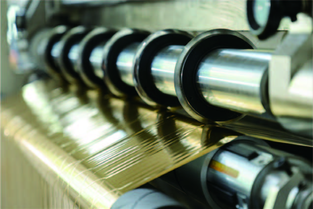
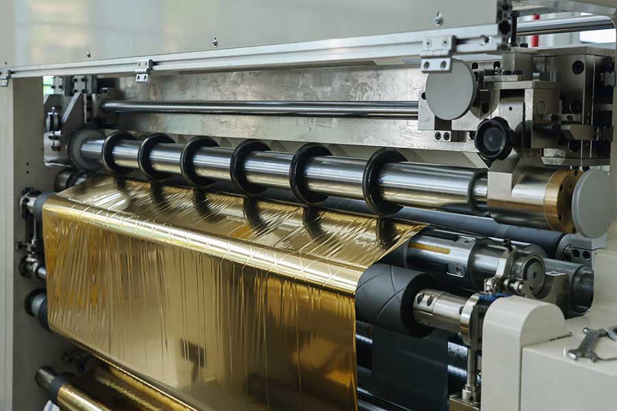
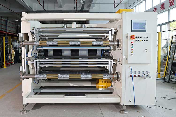
 Automatic Thermal Transfer Ribbon Slitting Machine RSDS8 H PLUS
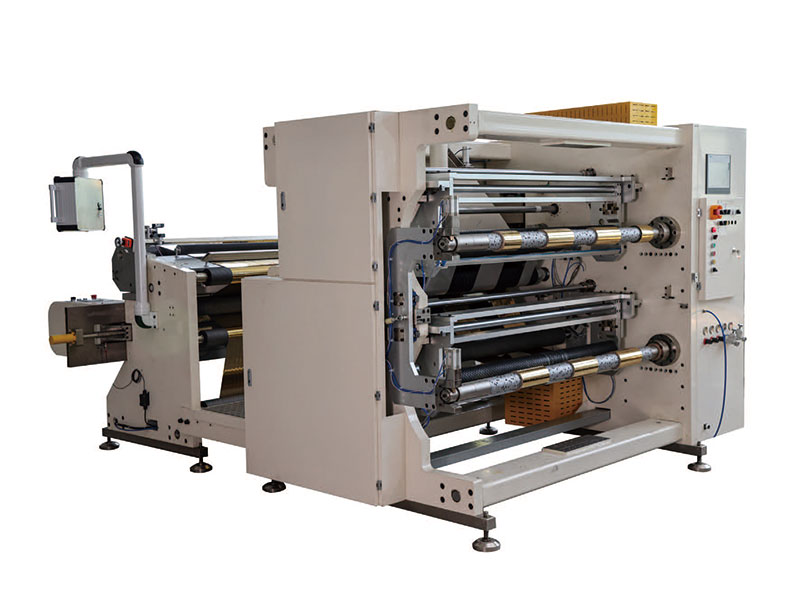 1400mm Hot Stamping Foil Slitting Machine
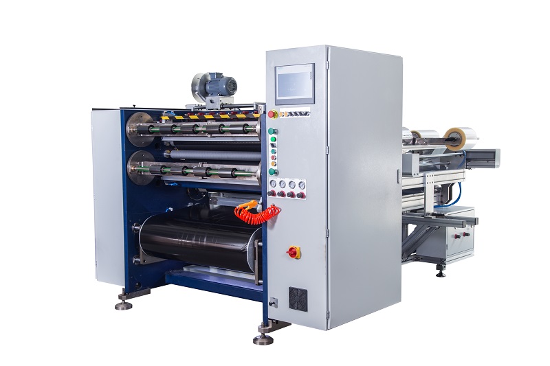 Semi Automatic Thermal Transfer Ribbon Slitting Machine RSDS5 PLUS
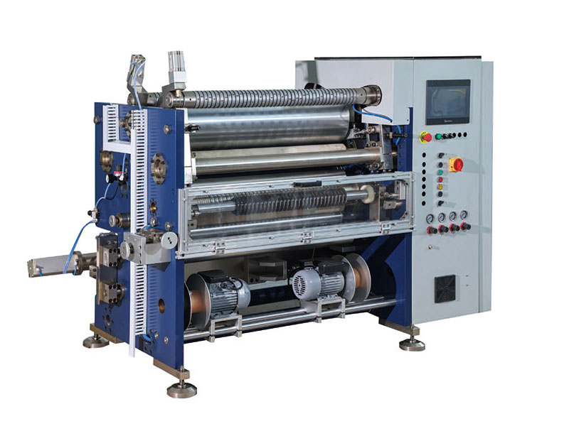 800mm Hot Stamping Foil Slitting Machine
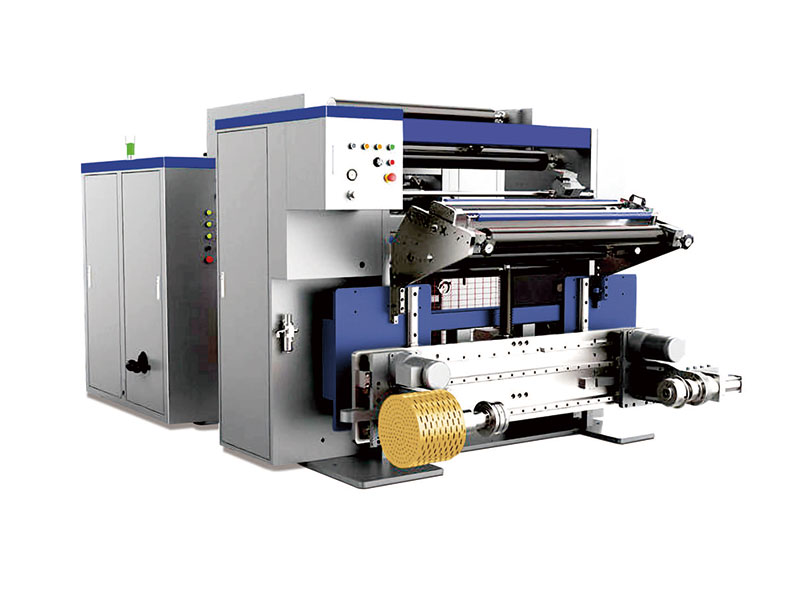 High Speed Slitting Machine
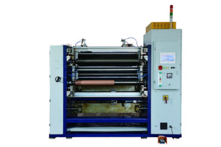 New Energy Ultra-thin Film Slitting Machine For Capacitive Film
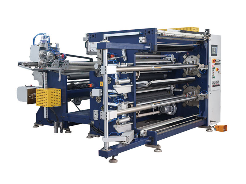 1350mm Hot Stamping Foil Slitting Machine
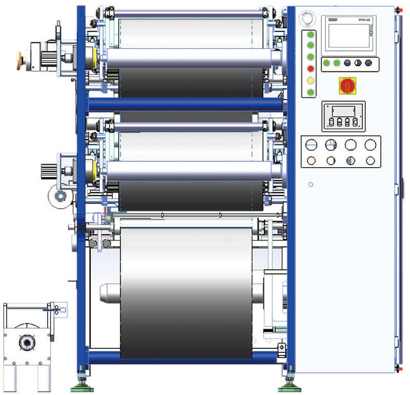 Customerized Slitter
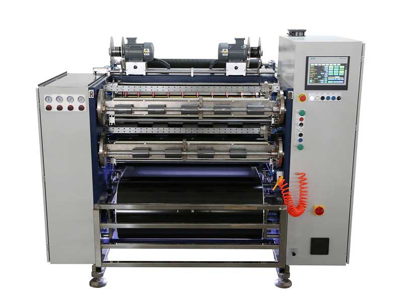


 +86 135 9951 7291
 support@delishmachine.com